2012-08-31

Tokyo court hands Samsung a win over Apple

Tokyo court hands Samsung a win over Apple


LONDON – A Tokyo court has found Samsung not guilty of infringing Apple's intellectual property, in contrast to a jury decision and a $1.05 billion damage award in Apple's favor in a California court last week.

Tokyo district court judge Tamotsu Shoji ruled Friday (Aug. 31) rejected Apple's claim that Samsung's products infringe patents related to synchronization of media files.

A week before a nine-person U.S. federal jury had found that many of Samsung's phones infringe most of two design and three utility patents held by Apple. However, the U.S. jury found that Samsung's tablets do not infringe Apple's iPad design patent.

"We welcome the court's decision, which confirmed our long-held position that our products do not infringe Apple's intellectual property," Reuters quoted Samsung as saying in a statement following the verdict from the Tokyo court.

The court case in Japan was not as broad as that conducted in the U.S., focusing only on a synchronization feature. Nonetheless it could have prevented the sale of Samsung Galaxy mobile phones, albeit older ones targeted by Apple, in Japan. The ruling leaves the way open for Samsung to continue selling smartphones in the Japanese market where it has been beating Apple in volume, the Financial Times said. Apple had been asking for comparatively modest damages of 100 million yen (about $1.3 million) the report said.

Unlike in South Korea and the United States, Japan rules case-by-case. Six other issues are yet to be ruled on by the Tokyo court, according to a Korea Times report. Samsung and Apple are also fighting in courts in Germany, Italy, the United Kingdom, France and the Netherlands.

The Japanese decision in favor of Samsung in Japan is likely to provide further encouragement for Samsung to appeal the U.S. decision. The U.S. judge set Sept. 20 as the date for hearing to determine whether to set an injunction against Samsung selling in the U.S. any of the products that court found to be infringing. Those products are generally a set of about 12 Samsung Galaxy S and S II handset models.


Related links and articles:

Reuters report

Apple awarded $1.05 billion in Samsung patent case

Apple versus Samsung questions on the Monday after

Jury foreman in Apple versus Samsung had 'light bulb moment'


TAG:Samsung Apple Tokyo court Galaxy

Samsung wins over Apple in Tokyo court

Samsung wins over Apple in Tokyo court


LONDON – A Tokyo court has found Samsung not guilty of infringing Apple's intellectual property, in contrast to the legal decision and the $1 billion ruling that went in favor of Apple and against Samsung in a California court last week.

Tokyo district court judge Tamotsu Shoji ruled Friday (Aug. 31) rejected Apple's claim that Samsung's products infringe patents related to synchronization of media files.

A week before a nine-person U.S. federal jury had found that many of Samsung's phones infringe most of two design and three utility patents held by Apple. However, the U.S. jury found that Samsung's tablets do not infringe Apple's iPad design patent.

"We welcome the court's decision, which confirmed our long-held position that our products do not infringe Apple's intellectual property," Reuters quoted Samsung as saying in a statement following the verdict from the Tokyo court.

The court case in Japan was not as broad as that conducted in the U.S., focusing only on a synchronization feature. Nonetheless it could have prevented the sale of Samsung Galaxy mobile phones, albeit older ones targeted by Apple, in Japan. The ruling leaves the way open for Samsung to continue selling smartphones in the Japanese market where it has been beating Apple in volume, the Financial Times said. Apple had been asking for comparatively modest damages of 100 million yen (about $1.3 million) the report said.

Unlike in South Korea and the United States, Japan rules case-by-case. Six other issues are yet to be ruled on by the Tokyo court, according to a Korea Times report. Samsung and Apple are also fighting in courts in Germany, Italy, the United Kingdom, France and the Netherlands.

The Japanese decision in favor of Samsung in Japan is likely to provide further encouragement for Samsung to appeal the U.S. decision. The U.S. judge set Sept. 20 as the date for hearing to determine whether to set an injunction against Samsung selling in the U.S. any of the products that court found to be infringing. Those products are generally a set of about 12 Samsung Galaxy S and S II handset models.


Related links and articles:

Reuters report

Apple awarded $1.05 billion in Samsung patent case

Apple versus Samsung questions on the Monday after

Jury foreman in Apple versus Samsung had 'light bulb moment'


TAG:Samsung Apple Tokyo court Galaxy

Samsung wins over Apple in Tokyo court

Samsung wins over Apple in Tokyo court


LONDON – A Tokyo court has found Samsung not guilty of infringing Apple's intellectual property, in contrast to the legal decision and the $1 billion ruling that went in favor of Apple and against Samsung in a California court last week.

Tokyo district court judge Tamotsu Shoji ruled Friday (Aug. 31) rejected Apple's claim that Samsung's products infringe patents related to synchronization of media files.

A week before a nine-person U.S. federal jury had found that many of Samsung's phones infringe most of two design and three utility patents held by Apple. However, the U.S. jury found that Samsung's tablets do not infringe Apple's iPad design patent.

"We welcome the court's decision, which confirmed our long-held position that our products do not infringe Apple's intellectual property," Reuters quoted Samsung as saying in a statement following the verdict from the Tokyo court.

The court case in Japan was not as broad as that conducted in the U.S., focusing only on a synchronization feature. Nonetheless it could have prevented the sale of Samsung Galaxy mobile phones, albeit older ones targeted by Apple, in Japan. The ruling leaves the way open for Samsung to continue selling smartphones in the Japanese market where it has been beating Apple in volume, the Financial Times said. Apple had been asking for comparatively modest damages of 100 million yen (about $1.3 million) the report said.

Unlike in South Korea and the United States, Japan rules case-by-case. Six other issues are yet to be ruled on by the Tokyo court, according to a Korea Times report. Samsung and Apple are also fighting in courts in Germany, Italy, the United Kingdom, France and the Netherlands.

The Japanese decision in favor of Samsung in Japan is likely to provide further encouragement for Samsung to appeal the U.S. decision. The U.S. judge set Sept. 20 as the date for hearing to determine whether to set an injunction against Samsung selling in the U.S. any of the products that court found to be infringing. Those products are generally a set of about 12 Samsung Galaxy S and S II handset models.


Related links and articles:

Reuters report

Apple awarded $1.05 billion in Samsung patent case

Apple versus Samsung questions on the Monday after

Jury foreman in Apple versus Samsung had 'light bulb moment'


TAG:Samsung Apple Tokyo court Galaxy
碧玉花瓶:漂洋过海终还乡

碧玉花瓶:漂洋过海终还乡

周勇锋收藏的碧玉花瓶. 肖亮 摄 周勇锋收藏的碧玉花瓶. 肖亮 摄 周勇锋向记者展示他收藏的碧玉碗. 肖亮 摄 周勇锋向记者展示他收藏的碧玉碗. 肖亮 摄

  实习生 胡谦 记者 田芳

  周勇锋的宝福堂,收藏的物件以大型的居多,柜台里摆放的众多大型和田白玉雕刻的物件能让你瞬间感受到一种大气.而在这么一大片白玉中间,两个碧玉物件可算是“白花丛中两点绿”.一个是碧玉碗,另一个便是碧玉花瓶了.碧玉碗以薄取胜,周身刻着金色诗文,碗底还有雍正年制的款识.而碧玉花瓶就略显神秘了,瓶身刻有一幅“江山览胜”图,亭台山水尽在其中.“这个碧玉花瓶是由一块完整的和田碧玉山料雕刻而成,缠枝莲纹的双耳、两边镂空的玉环都是整体的一部分,主要是雕刻人为显示自己的高超技艺.”周勇锋说.因为花瓶体形大、分量足,尽管瓶子内部是挖空的,但周勇锋搬起来还有点吃力.

  “碧玉花瓶是晚清的物件,是我两年前从日本古玩市场收购回来的.”周勇锋说.最开始,他主要是在福建、厦门、广州等沿海城市淘宝贝,后来全国各地都开始成为他的淘宝范围,五六年前则开始将目光转向国外.周勇锋解释:“主要是那时外国人对中国文化和中国古玩市场还不是特别了解,因此国外价格比国内低,所以很多中国人都去国外买中国古玩.但是现在反过来了,国外的价格甚至比国内还要高,去国外淘宝已经没什么空间了.”周勇锋强调,掌握好市场变化真的很重要.古玩市场是时刻变化的,近年来国内市场发展得比较好,和田玉升值很快,周勇锋几年前收购的和田玉物件现在价值都已经不是当时可以比拟的了.

  周勇锋是江西人,2000年来到长沙,有十多年的收藏经历.最开始他只是玩钱币,爱上收藏后,便瓷器、玉器、竹雕、牙雕都有接触.“以前跑货运赚的钱都投入到了收藏,家里人当时不大支持,但是后来也理解了.”周勇锋说.那个时候的周勇锋经常在清水塘逛地摊,他表示:“十年前淘地摊,好东西很多,好瓷器也遇到了不少.”

  玩古玩是一个渐进的过程,行内就有“三年瓷器,五年玉器,十年字画”的说法.周勇锋说,平时多看书、看实物、与玩家交流心得,不断学习,才能够慢慢掌握更多古玩知识,炼就火眼金睛.

  慧眼识宝

  和田碧玉“五德”助你辨真伪

  碧玉玉质的真伪,是玉器行生意成败的关键.玉质对了,即使时代上有误差,也不会血本无归,玉质错了,纵有千般理由,也是一亏到底.收藏者在受骗与反受骗的过程中,给和田碧玉总结了“五德”,即坚韧的质地、温润的光泽、绚丽的色泽、致密而透明的组织、舒扬致远的声音五大特征.通过“五德”可以找到和田碧玉简单有效的鉴别方法.

  一、划印法,把从外形上看颜色鲜亮、石质细润的玉件,用硬度为5.5至6的小钢刀划几下,毫无痕迹者可能是和田碧玉.

  二、玻璃法,用玉件角楞划磨硬度为5至5.5的玻璃,玻璃上出现痕迹的可能是和田碧玉.

  三、滴水法,由于和田碧玉密度高,将水滴上后,水滴边缘整齐而不扩散.

  四、手摸法,将玉件拿在手中,摸一摸,搓一搓,有温润、油滑之感.

  五、视察法,将玉朝后光明处,比如阳光或灯光处,凡颜色剔透、结构均匀者也可能是和田碧玉.


来源:新浪收藏
分享到: QQ空间 新浪微博 腾讯微博 人人网


TAG:碧玉花瓶:漂洋过海终还乡 翡翠 翡翠手镯 中国翡翠网 翡翠新闻

IWC海洋时计深海二号潜水员腕表 带来无尽深海世界的安全保障

IWC海洋时计深海二号潜水员腕表 带来无尽深海世界的安全保障

使用 探索深海的最佳伙伴 尽享深海世界的安全保障

IWC海洋时计深海二号潜水员腕表 带来无尽深海世界的安全保障

安全指示

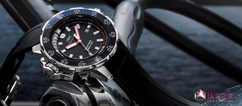
蓝色及红色指示器分别显示目前及最深的下潜深度

IWC海洋时计深海二号潜水员腕表 带来无尽深海世界的安全保障

加拉帕戈斯

防水深度达12巴

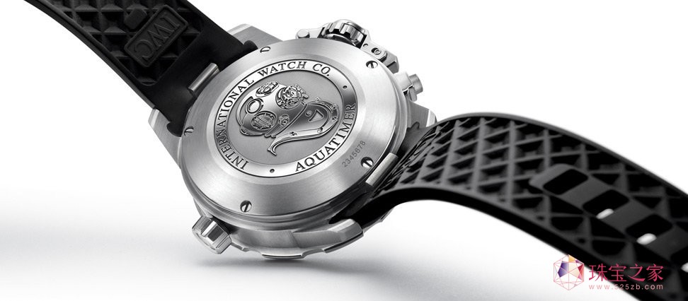
海洋时计深海二号潜水员腕表配备机械深度计,可提供最大的安全保障。这款腕表防水深达12巴,配有一套完整的备用系统,在潜水电脑失效的情况下,潜水员可以测量和设置重要参数,如潜水深度和时间。两个标示在白色刻度上显示潜水过程中的当前深度和最大深度(深达50米)。蓝色标示的移动显示实际潜水深度,而红色标示显示潜水过程中所达到最大深度处。压力测量系统位于表壳的左侧。海洋时计深海二号潜水员腕表配置46毫米厚的精钢表壳,内置30110型自动机芯,带有中央秒针、日期显示和42小时的动力储备功能。精钢表底饰以精心制作的潜水头盔凸纹雕刻。经过进一步改良的精钢表链现在也配备了双按钮安全表扣。


细节

IWC海洋时计深海二号潜水员腕表 带来无尽深海世界的安全保障

型号 IW354702

表壳物料 精钢

表带 黑色橡胶表带

表盘颜色 黑色

机芯 30110

机械机芯

自动上链

上满链可提供42小时动力储备

中央秒针附掣停装置

机械旋转外圈 配备追针标示的机械深度计可显示最大深度50米 指针、表盘及旋转外圈具有夜光涂层 旋入式表冠 双面防反光凸状蓝宝石玻璃表镜

防水深达12巴

表链快速更换系统** 表壳厚度15.5毫米 直径46毫米

**海洋时计表链快速更换系统由IWC万国表研发,专利授权来自卡地亚。


TAG:IWC 潜水员腕表 精钢表 自动机芯 动力储备

玉在身上戴玉德心中藏

玉在身上戴玉德心中藏

细说玉德 春秋时期,人们对玉的认识从感性走向理性,一些思想家给玉注入丰富的文化内涵。管仲认为玉具九德,孔子认为玉具十一德,因“君子比德于玉”的观点深入人心,君子佩玉成为一种时尚。玉德作为道德和行为规范深深地植根于人们心中,驱动人们崇玉、爱玉、佩玉,一代一代传承至今,它提醒每一个佩玉的人:不要忘了玉德。

  管子论玉九德

  夫玉之所贵者,九德出焉。夫玉温润以泽,仁也;邻以理者,知也;坚而不蹙,义也;廉而不刿,行也;鲜而不垢,洁也;折而不挠,勇也;瑕适皆见,精也;茂华光泽,并通而不相陵,容也;叩之,其音清扬彻远,纯而不殽,辞也。是以人主贵之,藏之为宝,剖以为符瑞,九德出焉。

  ——《管子·水地》

  孔子论玉十一德

  子贡问于孔子曰:“敢问君子,贵玉而贱珉者何也?为玉寡而珉之多与?”孔子曰:“非为珉之多故贱之也,玉之寡故贵之地。夫昔者,君子比德于玉焉。温润而泽,仁也;缜密以粟,知也;廉而不刿,义也;垂之如坠,礼也;叩之,其声清越以长,其终绌然,乐也;瑕不掩瑜,瑜不掩瑕,忠也;孚尹旁达,信也;气如白虹,天也;精神见于山川,地也;圭璋特达,德也;天下莫不贵者,道也。《诗》曰:‘言念君子,温其如玉’,故君子贵之也。”

  ——《礼记·聘义》

  许慎论玉五德

  玉,石之美者,有五德:润泽以温,仁之方也;鳃理自外,可以知中,义之方也;其声舒扬,专以远闻,智之方也;不挠而折,勇之方也;锐廉而不忮,洁之方也。

  ——《说文解字》

  爱玉,是中华民族一贯的传统。自古以来,玉深受历代统治者和各阶层民众的钟爱。这种执著甚至痴迷的爱历经八千年风雨变迁而始终不改。但经历了历史和时代的变迁以后,中国人爱玉的侧重点已发生了很大的变化,现代人的眼光集中在玉的经济价值和审美价值上,古人则对玉的文化内涵给予更多的关注。

  在古代,“君子无故,玉不去身”,所谓君子,是指有道德,有担当,有社会责任感的“大人”。古代的君子之所以一定要佩玉,是因为玉不仅是大自然的精华,还具备君子一般的品德,所以古语有说:“君子比德于玉焉。”那么,玉到底有哪些品德呢?

  管仲第一个总结玉德

  在春秋时期以前,人们对玉的认识基本上只停留在感性认识上,从春秋时期开始,古人对玉的认识就从感性走向理性,玉被赋予了丰富的文化内涵。历史上第一个对玉德进行系统论述的是春秋时期的政治家、思想家管仲。管仲是治国奇才,他辅佐齐桓公九合诸侯,一匡天下,著有《管子》一书。在《管子》中,他首次对玉德进行赞美,指出玉有九德。

  管仲说,玉所以贵重,是因为它表现出九种品德,温润而有光泽,是它的“仁”;清澈而有纹理,是它的“知”;坚硬不屈,是它的“义”;棱角分明而不伤人,是它的“行”;鲜明而不污垢,是它的“洁”;可折而不可屈,是它的“勇”;缺点和优点都表现出来,是它的“精”,华美的光泽相互渗透而不互相侵犯,是它的“容”;敲击起来,其声音清扬远闻,纯而不乱,是它的“辞”。所以君主把玉看得很贵重,把玉收藏起来作为宝贝,把玉剖开,制作成信物、吉祥物,以充分体现玉的九种品德。

  玉与儒家思想结缘

  孔子是我国古代文化的集大成者,他在管仲去世一百多年后,对玉德进行了更加深入的阐述,并在美玉上刻上了儒家思想的烙印。《礼记·聘义》记载,有一次,孔子的得意门生子贡问孔子:“请问君子,世人为什么把玉看得很贵重而不把珉(似玉的美石)看在眼里呢?是不是因为玉很少而珉很多呢?”孔子回答说:“非也,并不是因为珉多才看轻它,也不是因为玉少才看重它。从前,就有人把玉德比作君子品德。玉温润而有光泽,就是仁;玉质致密坚硬,就是智;玉有棱角而不伤人,就是义;玉沉重欲坠,就是礼;敲击玉器,其声音清越悠长,曲终时戛然而止,就是乐;玉瑕不掩瑜,瑜不掩瑕,就是忠;作为信物号令四方,就是信;玉的气质如虹,就是天;玉能体现山川的精神,就是地;玉制的圭璋用于礼仪,就是德;天下人都把玉看得很贵重,就是道。《诗经》中说:‘想念那位君子,是想念他的品德,他温润如玉’。所以君子一向重视玉。”

  可以说,孔子已把玉的文化含义发挥到极致,由于管仲、孔子的大力推崇,有力地推动了玉文化的发展,使玉在艺术品的地位几乎无与伦比。

  可能是担心管仲和孔子总结的玉德太多太复杂,一般人难以理解,东汉的许慎在《说文解字》中对玉德作了简化。按他的解释,玉有五德:温润是仁;通过表面的纹理可以知道里面的结构是义;声音悠扬远闻是智;可折不可屈是勇;锐利而不伤人是洁。

  “真玉”专指新疆和田玉

  众所周知,玉有不同的产地,种类繁多。虽然许慎说玉是“石之美者”,但古人心目中的玉是有所特指的。考古表明,大约从商代开始,玉的概念已开始集中到新疆和田玉上。在殷墟妇好墓出土的755件玉器中,绝大多数都是和田玉。到西周时,人们心目中的玉已经专指和田玉,其他所有似玉的美石均被称为“珉”,珉与玉有明确的区别,这从子贡和孔子的对话中就可以了解到。


TAG:

How Intel can use wireless charging to attack ARM

How Intel can use wireless charging to attack ARM


LONDON – Intel is gearing up to make its wireless resonant energy link (WREL) technology a supporting element to its mobile computing and communications offering.

IDT has announced that it has been selected by Intel to design and deliver transmit and receive ICs and to help deliver wireless charging reference designs for use in ultrabooks, PCs, smartphones, and stand-alone chargers.

That is well and good. Most of us probably think that carrying all those different wired chargers around and having to continually plug gadgets in to juice them up seems a little bit last century.

But Intel has always combined technology with business so, assuming that what the company has is any good, do not expect it to develop the technology and donate it to the world – or even to simply sell it to the world. It is my belief that Intel will be looking to obtain additional leverage from this technology.

Intel is the dominant supplier of processors for personal computers but is very much the Johnny-come-lately in mobile phones, smartphones and tablet computers where the ARM processor architecture, and ARM's ecosystem partners dominate.

So how could Intel use its wireless charging technology to leverage its leading position in computers and transfer it into the mobile sector?
Next: The gadget swarm is the gadget
TAG:Intel ARM Apple Android Samsung wireless charging Atom semiconductor

哈民忙哈史前聚落遗址出土大量玉器

哈民忙哈史前聚落遗址出土大量玉器

  8月26日,哈民忙哈考古史前聚落遗址工地传来消息,通过进一步地挖掘,工作人员又挖出三座房址,并在其中发现了大量的人骨和玉器.

  8月20—22日,本报连续刊登了《记者探访哈民忙哈史前聚落遗址》系列报道,文章以近距离直击考古工作的方式,向读者全面介绍了新石器时代遗址目前的发掘情况、考古工作人员的工作情况等.随着考古工作的持续进行,8月26日,考古工作人员又挖出三座房址,并在其中发现了大量的人骨和玉器.据考古工作人员阿茹娜介绍,发掘场面十分震撼,在之前两年的发掘过程中,我们也发现了一些玉器,但是数量不多,这次发现更增加了我们下一步发掘的信心.(记者李娜)


来源:新浪收藏
分享到: QQ空间 新浪微博 腾讯微博 人人网


TAG:哈民忙哈史前聚落遗址出土大量玉器 翡翠 翡翠手镯 中国翡翠网 翡翠新闻

赏玩和田玉需懂行和识货

赏玩和田玉需懂行和识货

  位于南京石头城84号贵人有玉坊馆长老怪得到天价羊脂玉的事传开后,老怪爱玉如痴的平静生活即被打乱.每天到其和田玉会馆请老怪帮忙掌眼买玉、咨询玉的价值的客人让老怪应接不暇.老怪感叹:在和田玉行业懂玉的行家实在是太少了.

  徐州做养生事业的张女士几年前因事业有成手中握有大量闲钱,再加上身边富起来的朋友圈几乎人手一玉甚至人手几玉,自视自己比朋友们智商高的她当年即去古玩玉石市场花费700余万元一口气买下11块看上去“挺不错”的和田玉原石,现在的张女士是让人一看即“珠光宝气”:手上戴着玉镯,胸前佩着金镶玉玉坠,就连她的奔驰汽车钥匙上也挂着小玉件,张女士前后在玉石上共投资了1600多万元.听着张女士滔滔不绝地述说她精彩的投资经历,再看看张女士带来的玉石,老怪实在不忍心对大老远从徐州赶来的张女士所携带的玉石加以评价,就热心地带着张女士参观欣赏了贵人有玉坊的很多和田玉藏品,并让她进行相互比较、比对欣赏以提高她对玉的鉴赏识别能力.看了贵人有玉坊的大量和田玉后,再回头看看自己身上所佩戴的玉器,以及携带的和田玉原石,张女士懊悔地说:“如果早认识老怪几年,就不会在和田玉投资道路上走弯路了.” 像张女士这样在玉石投资上走弯路的人很多.和田玉国之重器,被称为“国玉”,大凡富裕起来的成功人士都想以拥有几件和田玉来卓显自己的成功.老怪几年前就遇到一位在南京做地产的浙江商人陈先生曾让助手拎着耗资2000多万购买的两大包和田玉来请老怪给予鉴定和估价,当时老怪看了他的玉石后心里很不是滋味,因为当时这2000多万的玉石在老怪看来是500万也不敢接手的.

  识别和田玉,高深学问书本学不到

  老怪坦言,在玉石行业,没有绝对的专家,只有实战的行家,特别是和田玉,要想弄清和了解它的玉质差异,必须经过大量的玉石过手和不厌其烦地进行比较、切割、琢磨、研究,还要对玉找到感觉(俗称开悟),才能对玉有一定的认识,这些实战学问在书本是学不到的.每每对于各路藏家向他咨询玉的价值,老怪更是给出独到的见解:任何一块玉除了它本身的合理价值外,还会因为它在买卖双方之间相互转让过程中产生的情感也会无形中增大和降低它的价值,例如买卖双方之间相互珍惜、相互信任、相互真诚,就会提升被买卖转让玉石的潜在身价,反之,老怪认为就是再好的玉石也会丢失一些玉石应有的灵气,同样它的价值也会随之大打折扣.

  正是因为以上的种种事例,老怪怀着一颗虔诚的心,从“君子比德于玉”的先人遗风出发,在南京石头城84号投资贵人有玉坊专业和田玉会所,以期让爱玉的人不再走弯路.更希望天下所有爱玉之人在贵人有玉坊这里能提升对玉的辨别能力和买到真正的和田玉、好的和田玉.

  苍 萍


来源:新浪收藏
分享到: QQ空间 新浪微博 腾讯微博 人人网


TAG:赏玩和田玉需懂行和识货 翡翠 翡翠手镯 中国翡翠网 翡翠新闻

2012-08-30

和田玉的形成与类型

和田玉的形成与类型

  收藏知识

  中国人认为玉是通人性的,所以有“通灵宝玉”之说.和田玉是如何形成的,又有何特征呢?

  一、和田玉的产地之源

  和田玉目前有两个著名的产玉之源:一个就是从新疆于田县向南,进入昆仑山脉,那里有一个著名的阿拉玛斯矿区,现在最著名的和田白玉山料就产于此.另外一个就是由和田市往南,沿白玉河溯源而上.那里就是盛产历史悠久的籽儿玉、山流水料的源头.流经新疆和田境内的河流有两条:一个叫玉龙喀什河,一个叫喀拉喀什河.数亿年前每当洪水过后,就会从昆仑山上冲下来许多珍贵的玉石.

  二、和田玉的形成之秘

  和田玉按照产出地的不同,可分为:山料、山流水、籽料三种类型.

  1、山料:即通过玉矿开采的玉石,主要产在昆仑山中.有的矿井灌进雨雪,形成晶莹碧透的冰洞.洞被炸开后,就沿着蓝色的玉线寻找玉石.玉石不是集中在一起,而是鸡窝状,一般包裹在大理石中,需要进行剥离.

  2、山流水:名称是由采玉和琢玉艺人命名的.它是原生玉矿石经风化崩落,并由河水冲击至河流中上游而形成的玉石.山流水的特点是距原生矿近,块度较大,棱角稍有磨圆,表面较光滑,年代稍久远,比籽玉年轻.

  3、籽料:是由山料,经冰川不断裂解崩落,地震风化或被洪水冲入河道并受到河水的长期碰撞侵蚀经千万年所形成,其形如鹅卵,质地细糯;滋润,密度大,多有皮色,为玉中珍品.而籽玉中最珍贵的白玉是羊脂玉,可以这样说,现在就是有钱,也不一定能买到精绝之品羊脂玉.而现如今自称羊脂玉的,其实大多数是高白色的山玉料.

  综上所述,玉料是玉器收藏的首要前提,行家多看重籽料,尤其带皮上品特等籽料更是可遇而不可求.和田玉器的市场价格分析:羊脂玉最高、籽料高、山流水次之、山料更次之.

  阳洋


来源:新浪收藏
分享到: QQ空间 新浪微博 腾讯微博 人人网


TAG:和田玉的形成与类型 翡翠 翡翠手镯 中国翡翠网 翡翠新闻

翡翠收藏看重原料还是工艺

翡翠收藏看重原料还是工艺

  中华古玩网讯:原料还是工艺?收藏翡翠更注重哪项?首先还是要看料.拿到一件翡翠,外行看到的就是一件翠佛,或一颗戒面,或一个翡翠福豆;而同一件东西,行家看到的首先是一块翠料,它为什么会做成翠佛、戒面、福豆,完全是由翠料决定的.

  很多人都问我,翡翠行业为什么不像白玉那样有很多著名的工艺大师.其实翡翠行也有很多非常优秀的工艺师,但行里有句老话,叫“原料是师傅”.

  加工翡翠的工艺师,拿到一块翡翠,首先要做的第一件事,就是琢磨这件翠料.多年之前一位老师傅告诉我,他曾经雕一件翡翠,雕之前他对这块翠料“相面”整整相了两个月,天天把翡翠放在床头,白天起来第一眼,每晚睡前,都要看看这块翠料,他在等着翠料跟他讲话,告诉他应该做什么.

  同样是玉器,同样是雕琢,翡翠和白玉为什么不同呢?最重要之处在于,白玉雕刻中,除少数带糖皮的或墨玉白玉做俏雕以外,一件白玉成品中玉色、玉质变化的极少.翡翠原料颜色和玉质变化极大,即使在一件成品中,也常常有很多颜色,质地也会发生变化.所以工艺师不能完全任由自己设计,翡翠加工的最高境界就是把翠料的美尽可能地表现出来,并使璞玉的价值得到最高实现.

  工艺也重要,一件好的翠料绝不会找差的工.好的工艺一定能把翠料的天然之美表现得最好,天人合一.看一件翡翠的价值,看一件翡翠是否值得收藏,就不能仅像大多数行家那样,仅把翡翠看成原料,更应把它看成一件艺术品,只有工艺和原料结合得最好的翡翠,才是最有升值空间的,这也是鉴赏一件翡翠的最高层次.

  普通收藏者如果对翡翠的真假没有把握,当你看到一件种好色艳的翡翠,却有着粗糙的工艺,基本就可以断定这是一件赝品.判定翡翠真伪对普通人来说很难,但看一件翡翠工艺的审美,是大多数人都能做到的,因此这个方法也是初入行者看翠的一个小窍门.

  (注:本文作者万女士系万瑞祥翡翠俱乐部首席鉴赏专家、国家注册珠宝评估师)


来源:新浪收藏
分享到: QQ空间 新浪微博 腾讯微博 人人网


TAG:翡翠收藏看重原料还是工艺 翡翠 翡翠手镯 中国翡翠网 翡翠新闻

Formosa Plastics bails out DRAM subsidiaries

Formosa Plastics bails out DRAM subsidiaries


LONDON – Formosa Plastics Group, parent of Nanya Technology Corp., has put together a bail-out plan worth about $1 billion to keep the loss-making DRAM maker from delisting from the Taiwan stock exchange, according to local reports.

Nanya has been struggling for a number of years but the bail-out plan is being taken as evidence that the Formosa Plastics Group (FPG) is determined to stay in the semiconductor business.

Four firms within FPG – Formosa Plastics Corp., Formosa Petrochemical Corp., Formosa Chemicals & Fiber Corp. and Nanya Plastics Corp. – will provide Nanya Technology with total of NT$29.6 billion (about $990 million). The four companies will each provide NT$7.4 billion (about $247 million), the reports said.

At the same time Formosa Petrochemical has approved the lending of NT$4.8 billion (about $160 million) to Inotera Memories Inc., according to a Taipei Times report. Inotera is a joint venture between Nanya Technology and Micron Technology Inc. (Boise, Idaho).

FPG had annual sales in 2011 of $74.7 billion on which it made a profit before tax of $4.7 billion.


Related links and articles:

www.fpg.com.tw

www.nanya.com

Related links and articles:


Elpida's bankruptcy to boost other DRAM suppliers

Micron increasing stake in Inotera

Report: Nanya to get billion-dollar boost


TAG:Formosa Plastics Group FPG Nanya Inotera Micron memory semiconductor DRAM

Formosa Plastics bails out DRAM subsidiaries

Formosa Plastics bails out DRAM subsidiaries


LONDON – Formosa Plastics Group, parent of Nanya Technology Corp., has put together a bail-out plan worth about $1 billion to keep the loss-making DRAM maker from delisting from the Taiwan stock exchange, according to local reports.

Nanya has been struggling for a number of years but the bail-out plan is being taken as evidence that the Formosa Plastics Group (FPG) is determined to stay in the semiconductor business.

Four firms within FPG – Formosa Plastics Corp., Formosa Petrochemical Corp., Formosa Chemicals & Fiber Corp. and Nanya Plastics Corp. – will provide Nanya Technology with total of NT$29.6 billion (about $990 million). The four companies will each provide NT$7.4 billion (about $247 million), the reports said.

At the same time Formosa Petrochemical has approved the lending of NT$4.8 billion (about $160 million) to Inotera Memories Inc., according to a Taipei Times report. Inotera is a joint venture between Nanya Technology and Micron Technology Inc. (Boise, Idaho).

FPG had annual sales in 2011 of $74.7 billion on which it made a profit before tax of $4.7 billion.


Related links and articles:

www.fpg.com.tw

www.nanya.com

Related links and articles:


Elpida's bankruptcy to boost other DRAM suppliers

Micron increasing stake in Inotera

Report: Nanya to get billion-dollar boost


TAG:Formosa Plastics Group FPG Nanya Inotera Micron memory semiconductor DRAM

Intel energizes wireless charging effort

Intel energizes wireless charging effort


LONDON – Intel has selected mixed-signal fabless chip company Integrated Device Technology Inc. to make an transmitter and receiver ICs for Intel's resonant wireless energy transfer technology.

Intel (Santa Clara, Calif.) is pushing hard to bring the technology to market to improve the attractiveness of mobile offerings based on its processors such as Intel-based ultrabooks and smartphones. Intel has been developing resonant wireless charging since before October 2008.

IDT (San Jose, Calif.) said it plans to be able to provide samples the resonance receiver IC by the end of 2012 and the year, and of the transmitter IC sometime in the first half of 2013. Intel and IDT also plan to deliver resonant wireless charging reference designs for use in Ultrabooks, PCs, smartphones, and standalone chargers.

Wireless charging over distances of a few millimeters or centimeters using magnetic induction has been seen as a promising application area for a number of years but has been difficult to find an efficient means of energy transfer and consensus on standards has been slow to build.

"Our extensive experience in developing the innovative and highly integrated IDTP9030 transmitter and multi-mode IDTP9020 receiver has given IDT a proven leadership position in the wireless power market,” said Arman Naghavi, vice president and general manager of the analog and power division at IDT, in a statement.

"We think the ability to have a wire-free charging experience with a broad ecosystem of devices like keyboards, mice, storage devices, cameras and smartphones will be realized in the near future," said Gary Huang, director of PC growth and innovation at Intel, in the same statement.


Related links and articles:

www.wirelesspowerbyidt.com

Intel video demo

www.wirelesspowerconsortium.com

News articles:

Intel preps wireless charging

Ti offers 'Qi' inductive power transfer IC

EE Times' 20 hot technologies for 2012

Silicon 60 v13.0


TAG:Intel IDT wireless resonant charging energy transfer semiconductor

London Calling: Recore and will.i.am

London Calling: Recore and will.i.am


LONDON – What do Recore Systems BV and William Adams, otherwise known as rapper will.i.am, have in common?

Recore Systems (Enschede, The Netherlands), a 2005 fabless startup, has recently presented a reliable data processor to the European Space Agency.

Recore's FPGA-based prototype dubbed MPPB (Massively Parallel Processor Breadboarding system, ESA contract 21986) includes reconfigurability techniques in support of fault tolerance.

Recore develops parallel reconfigurable digital signal processing intellectual property around its Montium and Xentium accelerator cores and the company was asked to produce a reliable processor by the European Space Research and Technology Centre (Noordwijk, The Netherlands) part of the European Space Agency.

Data processing on-board spacecraft and satellites is subject to high radiation levels and European rad-hard DSPs lack the performance needed for future applications.

"We introduced our concepts of self-repairing reconfigurable chips to ESA in 2009, and explained that a multicore system can detect which parts of hardware are faulty and then can continue to process data with the healthy cores," said Gerard Rauwerda, CTO at Recore, in a statement. "ESA contracted us to embed it in a prototype with proven space concepts such as Leon processors and space-standard interfaces such as SpaceWire."


Click on image to enlarge.

MPPB systems architecture with Xentium DSPs and proven space components and interfaces. Source: Recore.

Next: Intel's man
TAG:Peter Clarke Recore Systems William Adams will i am IBC Amsterdam

Slideshow: Novel server CPUs glow at Hot Chips

Slideshow: Novel server CPUs glow at Hot Chips

SAN JOSE, Calif. – In the next five years, ARM-based SoCs will grab about ten percent of the server market, according to a straw poll of engineers at the annual Hot Chips. ARM’s future in the data center was a hot topic of debate in an afternoon session dedicated to a smorgasbord of next-generation server processors.

In a keynote kicking off the session, former Intel chief technology officer Patrick Gelsinger said ARM will maintain dominance in mobile systems but won’t gain a foothold in data centers. The x86 makes up more than 95 percent of all server units and 70 percent of server CPU revenues, he said.

“It’s is the only architecture that matters, and we are betting heavily on this being the computing architecture for the data center,” said Gelsinger (below) who is a division president of storage giant EMC and set to become chief executive of its VMWare subsidiary on September 1.


TAG:Hot Chips ARM Servers X86 Processors IBM Oracle Fujitsu Power7+ Sparc ZNext Applied Gelsinger

Slideshow: Novel server CPUs glow at Hot Chips

Slideshow: Novel server CPUs glow at Hot Chips

SAN JOSE, Calif. – In the next five years, ARM-based SoCs will grab about ten percent of the server market, according to a straw poll of engineers at the annual Hot Chips. ARM’s future in the data center was a hot topic of debate in an afternoon session dedicated to a smorgasbord of next-generation server processors.

In a keynote kicking off the session, former Intel chief technology officer Patrick Gelsinger said ARM will maintain dominance in mobile systems but won’t gain a foothold in data centers. The x86 makes up more than 95 percent of all server units and 70 percent of server CPU revenues, he said.

“It’s is the only architecture that matters, and we are betting heavily on this being the computing architecture for the data center,” said Gelsinger (below) who is a division president of storage giant EMC and set to become chief executive of its VMWare subsidiary on September 1.


TAG:Hot Chips ARM Servers X86 Processors IBM Oracle Fujitsu Power7+ Sparc ZNext Applied Gelsinger

AlcaLu CTO calls for new basestation chips

AlcaLu CTO calls for new basestation chips

CUPERTINO, Calif. – Tomorrow’s wireless networks need chips designed mainly for a new class of small-cell basestations that will serve the growing capacity needs of mobile data users. But just where the money needed to build the new networks will come from is unclear.

That was the message Marcus Weldon, chief technology officer at Alcatel-Lucent, delivered to several hundred processor designers at the annual Hot Chips conference here.

“We are in a radical transition to a capacity-driven world served by Wi-Fi and small cells and away from a coverage world” using macro cellular basestations, Weldon said. “All the new chip set designs will have a focus on metro cells with a smaller emphasis on macro cells,” he said.

“Small cells are the only way to get 80-fold factor in additional capacity that will be needed,” he added.

Weldon predicted as many as 500 million tablet computers will be sold each year by 2017. They will, along with the rise in smartphones, drive the 80-fold increase in mobile data next-generation wireless networks will need to serve.

The needs are rising at a time when carrier’s data revenues are relatively flat and their voice revenues are falling. He suggested carriers will look for ways to charge per connection and per service, especially for new ways of shifting into the digital realm traditional “analog” jobs in banking, health care and other domains.

“We are in a staring match between content and network people where no one has figured out the model to build the network with the money in the pot,” said Weldon, pictured below. “It’s the entire digital economy wallet we should look at,” he said.


TAG:Small Cell Basetations Small Cells Metro Cells Hot Chips Alcatel Lucent Basestations Cavium Freescale

国内最大玉雕插牌《清明上河图》完工

国内最大玉雕插牌《清明上河图》完工

碧玉大型插牌《清明上河图》 碧玉大型插牌《清明上河图》

  昨日,记者从玉石料市场田翔工作室获悉,碧玉大型插牌《清明上河图》日前已全部完工.据介绍,这件作品是目前国内体量最大的一件玉器插牌.目前保守估价不会低于1000万.

  玉 料

  10吨碧玉上最好的一块

  “这件作品的原材料就值500万元,而且这么好的加拿大碧玉可遇而不可求,很多时候有再多钱也买不到.”江苏省工艺美术大师、《清明上河图》的主要设计制作者田翔,对当初与这块玉料的相遇记忆犹新.

  今年上半年,扬州工艺美术集团的多位工作人员远赴加拿大,直接采购回一块10吨重的加拿大碧玉.“能找到这么大的原材料非常难得,更何况整块材料通体碧绿,我一见到它就爱不释手.”

  10吨的原材料自然不可能只做一件作品.因此切割它费了一番周折.“既要切得平整,又要得材率高.可是扬州没有这么大的切割工具,只得运往河南操作,切割后再运回扬州.”田翔说,《清明上河图》的这块料约重200公斤,是所有切割后的玉料中品质最好的.“它的绿色纯正得诱人,几乎找不到一点瑕疵,也看不见一个黑点杂质.”

  作 品

  200多个人物神态各不相同

  “一拿到这块玉料,我们就被告知这件作品的目标是今年的西博会,所以在琢磨这块玉料做什么的时候我们既要谨慎又要大胆.”田翔说,《清明上河图》是较为常见的工艺题材,但是因为其是平面的画稿,所以最适合的表现手法莫过于刺绣.可是为了打破常规,负责这件作品题材策划的“国大师”薛春梅最终和他们一锤定音,“这件玉器插牌就做《清明上河图》,而且是其中最经典的一段《虹桥漕运》.”

  整件作品长200厘米,宽80厘米,厚度达到4厘米,是目前国内最大的一件玉器插牌作品.作品中共涉及200余个人物,其中,有衣着光鲜的官员、有腰缠万贯的商贩、有正在劳作的民工,还有穿梭于街巷中的普通百姓.

  “整件作品表现了宋代轻松、安逸的市井生活.200多个人物的服饰打扮都与各自的身份相切合.不但每个人的神态各不相同,而且人与人之间还有一定的表情、动作相呼应.”记者留意到,桥头有人招手,桥下必有人应和;街边有人吆喝买卖,周围也必定有人讨价还价……

  变平面画稿为立体玉雕

  难 度

  传统的中小型插牌都是以山水为主,可这件大体量的插牌却破天荒地选择了一个动态的生活场景,其中有人、有建筑、有树木流水、还有桥梁船只等.“因此雕琢的难度可想而知.”

  虽然有现成的画稿,但是如何将一幅平面的国画演变成一件立体的玉器插牌作品,成了田翔他们这个制作团队三个多月来每天都需要解决的问题.

  “一般的玉雕插牌的雕刻厚度在0.5厘米—2厘米之间,可是这件作品的雕刻厚度却在1.8厘米—2.5厘米之间.一半以上的人物都重叠在一起,而且至少两层以上,这更是在画面立体感上增加了难度,不过倒也更增添了工艺性和美感.”田翔说,制作时有好几位“国大师”与玉器行家都来看过,大家都对这种立体的布局很满意,可是也都担心难以表现.不过现在制作完成了,效果比预想的还要好.“用我们的行话说,处处都‘推拿’得恰到好处.”

  时 间

  2年工期缩短至97天完成

  据了解,这么大的玉器插牌作品正常完成需要2年时间,可是为了赶工期,这件《清明上河图》必须在3个月内赶制出来.“我从事玉雕工作整整33年,可以说这件作品是我做得最累,但也是最满意的.”回忆起这次制作过程,田翔感慨颇深.

  每天早晨7点45分,田翔和他的徒弟,还有技师赵跃健就会准时坐上操作台,除去午饭和晚饭时间,直到晚上11点,他们才会走出工作室.田翔说,他在新华书店内翻遍了与宋代市井生活相关的各种书籍和图册,就是为了更好地拿捏作品中的人物和建筑.而在制作中,为了表现得更加逼真,他们会时刻观察身边形形色色的陌生人,将他们在街头巷尾不经意间的言行举止转移到作品中.

  “因为工期太紧,不允许我们对作品设计有太大的改动,所以第二天的雕琢内容,基本上都是在前一天才刚刚敲定的.”田翔说,整整97天,他们三个制作者几乎一坐下就能睡着,而今天他们也终于能睡个整觉了.

  记者 安琪

  【读报词典】

  插 牌

  是玉雕的一个品类和表现形式,多镶嵌在墙上或用木质底座作托陈列观赏.是和山子雕、饰品、把玩件并列的一种玉器类型.


来源:新浪收藏
分享到: QQ空间 新浪微博 腾讯微博 人人网


TAG:国内最大玉雕插牌《清明上河图》完工 翡翠 翡翠手镯 中国翡翠网 翡翠新闻

AlcaLu CTO calls for new basestation chips

AlcaLu CTO calls for new basestation chips

CUPERTINO, Calif. – Tomorrow’s wireless networks need chips designed mainly for a new class of small-cell basestations that will serve the growing capacity needs of mobile data users. But just where the money needed to build the new networks will come from is unclear.

That was the message Marcus Weldon, chief technology officer at Alcatel-Lucent, delivered to several hundred processor designers at the annual Hot Chips conference here.

“We are in a radical transition to a capacity-driven world served by Wi-Fi and small cells and away from a coverage world” using macro cellular basestations, Weldon said. “All the new chip set designs will have a focus on metro cells with a smaller emphasis on macro cells,” he said.

“Small cells are the only way to get 80-fold factor in additional capacity that will be needed,” he added.

Weldon predicted as many as 500 million tablet computers will be sold each year by 2017. They will, along with the rise in smartphones, drive the 80-fold increase in mobile data next-generation wireless networks will need to serve.

The needs are rising at a time when carrier’s data revenues are relatively flat and their voice revenues are falling. He suggested carriers will look for ways to charge per connection and per service, especially for new ways of shifting into the digital realm traditional “analog” jobs in banking, health care and other domains.

“We are in a staring match between content and network people where no one has figured out the model to build the network with the money in the pot,” said Weldon, pictured below. “It’s the entire digital economy wallet we should look at,” he said.


TAG:Small Cell Basetations Small Cells Metro Cells Hot Chips Alcatel Lucent Basestations Cavium Freescale

2012-08-29

AMD appoints ecosystem expert to its board

AMD appoints ecosystem expert to its board


LONDON – Advanced Micro Devices Inc. has appointed Jack Harding, CEO of design and manufacturing services provider eSilicon Corp., to its board of directors.

The moves marks yet another step in a substantial shake up of the technical and business culture at the top of AMD (Sunnyvale, Calif.) by CEO Rory Read, who was appointed one year ago.

Harding co-founded eSilicon (Sunnyvale, Calif.) in 2000 after leaving EDA company Cadence Designs Systems Inc. where he had also served as CEO. Harding's recent experience at eSilicon has fostered expertise in the fabless and intellectual property ecosystems where AMD looks set to play. Harding has more than 25 years of management experience in the semiconductor industry, especially in the area of ASIC and system-on-chip design and manufacturing.

"Jack's wealth of industry experience and familiarity with evolving industry trends make him a perfect choice to join the AMD board," said AMD chairman Bruce Claflin, in a statement. "As AMD establishes itself as a more nimble, flexible semiconductor design innovator, Jack's operational experience, strategic expertise and business acumen for bringing SoC and custom integrated circuit solutions to market should add tremendous value for AMD's future business."

Before co-founding eSilicon, Harding joined Cadence when it acquired his former employer, Cooper & Chyan Technology. Harding has also held a variety of senior management positions at Zycad and IBM. Harding also serves on the board of directors of RF Micro Devices and the Global Semiconductor Alliance (GSA).


Related links and articles:

AMD lands high-performance computing guru

ESilicon set to reap rewards of Asian gamble

AMD names new sales chief

TAG:Jack Harding AMD eSilicon semiconductor processor SOC design Cadence

AMD appoints ecosystem expert to its board

AMD appoints ecosystem expert to its board


LONDON – Advanced Micro Devices Inc. has appointed Jack Harding, CEO of design and manufacturing services provider eSilicon Corp., to its board of directors.

The moves marks yet another step in a substantial shake up of the technical and business culture at the top of AMD (Sunnyvale, Calif.) by CEO Rory Read, who was appointed one year ago.

Harding co-founded eSilicon (Sunnyvale, Calif.) in 2000 after leaving EDA company Cadence Designs Systems Inc. where he had also served as CEO. Harding's recent experience at eSilicon has fostered expertise in the fabless and intellectual property ecosystems where AMD looks set to play. Harding has more than 25 years of management experience in the semiconductor industry, especially in the area of ASIC and system-on-chip design and manufacturing.

"Jack's wealth of industry experience and familiarity with evolving industry trends make him a perfect choice to join the AMD board," said AMD chairman Bruce Claflin, in a statement. "As AMD establishes itself as a more nimble, flexible semiconductor design innovator, Jack's operational experience, strategic expertise and business acumen for bringing SoC and custom integrated circuit solutions to market should add tremendous value for AMD's future business."

Before co-founding eSilicon, Harding joined Cadence when it acquired his former employer, Cooper & Chyan Technology. Harding has also held a variety of senior management positions at Zycad and IBM. Harding also serves on the board of directors of RF Micro Devices and the Global Semiconductor Alliance (GSA).


Related links and articles:

AMD lands high-performance computing guru

ESilicon set to reap rewards of Asian gamble

AMD names new sales chief

TAG:Jack Harding AMD eSilicon semiconductor processor SOC design Cadence

AMD appoints ecosystem expert to the board

AMD appoints ecosystem expert to the board


LONDON – Advanced Micro Devices Inc. has appointed Jack Harding, CEO of design and manufacturing services provider eSilicon Corp., to the board of directors.

The moves marks yet another step in a substantial shake up of the technical and business culture at the top of AMD (Sunnyvale, Calif.) by CEO Rory Read, who was appointed one year ago.

Harding co-founded eSilicon (Sunnyvale, Calif.) in 2000 after leaving EDA company Cadence Designs Systems Inc. where he had also served as CEO. Harding's recent experience at eSilicon has fostered expertise in the fabless and intellectual property ecosystems where AMD looks set to play. Harding has more than 25 years of management experience in the semiconductor industry, especially in the area of ASIC and system-on-chip design and manufacturing.

"Jack's wealth of industry experience and familiarity with evolving industry trends make him a perfect choice to join the AMD board," said AMD chairman Bruce Claflin, in a statement. "As AMD establishes itself as a more nimble, flexible semiconductor design innovator, Jack's operational experience, strategic expertise and business acumen for bringing SoC and custom integrated circuit solutions to market should add tremendous value for AMD's future business."

Before co-founding eSilicon, Harding joined Cadence when it acquired his former employer, Cooper & Chyan Technology. Harding has also held a variety of senior management positions at Zycad and IBM. Harding also serves on the board of directors of RF Micro Devices and the Global Semiconductor Alliance (GSA).


Related links and articles:

AMD lands high-performance computing guru

ESilicon set to reap rewards of Asian gamble

AMD names new sales chief

TAG:Jack Harding AMD eSilicon semiconductor processor SOC design Cadence

Report: TSMC rebuffs Apple, Qualcomm

Report: TSMC rebuffs Apple, Qualcomm


LONDON – Apple and Qualcomm have each offered more than a $1 billion to foundry Taiwan Semiconductor Manufacturing Co. to obtain a dedicated supply of processor chips, and both their offers have been rejected, according to a Bloomberg report.

Apple needs the chips for its own smartphomes and tablet computers – iPhones and iPads – while Qualcomm is the leading supplier of application processors to the rival Android platform of mobile equipment. Both the Apple and Qualcomm proposals included investments in TSMC (Hsinchu, Taiwan), Bloomberg said quoting unnamed sources.

At present Apple relies on Samsung Electronics Co. Ltd. for its leading edge A5 processor but Apple is in a high profile legal dispute with Samsung over the look and feel of smartphones. Apple has been reported to be working with TSMC (Hsinchu, Taiwan) to bring up a 28-nm A6 processor. Meanwhile Qualcomm, which has designed the Snapdragon processor, is known to be suffering from a shortage of supply at the 28-nm node.

There has been speculation that companies such as Apple and Qualcomm would try to use their financial muscle to obtain a secure supply of leading-edge chips which at present is limiting sales of mobile equipment.

In July Morris Chang, chairman and CEO of TSMC, said the company was considering operating single-customer wafer fabs so a rejection of the Apple and Qualcomm investment proposals may have resulted from detailed terms or the fact that equity was being sought.

However, as a foundry supplier TSMC profits from serving many fab-lite and fabless chip companies, including Broadcom, Nvidia, MediaTek and many others. If it was seen to be too close to Qualcomm or Apple it might risk its independent status and drive other customers into the arms of rival foundry suppliers.

In addition Lora Ho, chief financial officer of TSMC, has expressed reservations about operating single-customer wafer fabs. "You have to be careful. Once that product migrates, what are going to do with that dedicated fab? We would like to keep the flexibility," the Bloomberg report quoted Ho as saying.


Related links and articles

Bloomberg article


TSMC says single-customer fabs make sense

TSMC tops pure-play MEMS foundry ranking from IHS


Qualcomm sees 28-nm capacity crunch through 2012


On Qualcomm's manufacturing options


TAG:TSMC Apple Qualcomm processor semiconductor foundry

Report: TSMC rebuffs Apple, Qualcomm

Report: TSMC rebuffs Apple, Qualcomm


LONDON – Apple and Qualcomm have each offered more than a $1 billion to foundry Taiwan Semiconductor Manufacturing Co. to obtain a dedicated supply of processor chips, and both their offers have been rejected, according to a Bloomberg report.

Apple needs the chips for its own smartphomes and tablet computers – iPhones and iPads – while Qualcomm is the leading supplier of application processors to the rival Android platform of mobile equipment. Both the Apple and Qualcomm proposals included investments in TSMC (Hsinchu, Taiwan), Bloomberg said quoting unnamed sources.

At present Apple relies on Samsung Electronics Co. Ltd. for its leading edge A5 processor but Apple is in a high profile legal dispute with Samsung over the look and feel of smartphones. Apple has been reported to be working with TSMC (Hsinchu, Taiwan) to bring up a 28-nm A6 processor. Meanwhile Qualcomm, which has designed the Snapdragon processor, is known to be suffering from a shortage of supply at the 28-nm node.

There has been speculation that companies such as Apple and Qualcomm would try to use their financial muscle to obtain a secure supply of leading-edge chips which at present is limiting sales of mobile equipment.

In July Morris Chang, chairman and CEO of TSMC, said the company was considering operating single-customer wafer fabs so a rejection of the Apple and Qualcomm investment proposals may have resulted from detailed terms or the fact that equity was being sought.

However, as a foundry supplier TSMC profits from serving many fab-lite and fabless chip companies, including Broadcom, Nvidia, MediaTek and many others. If it was seen to be too close to Qualcomm or Apple it might risk its independent status and drive other customers into the arms of rival foundry suppliers.

In addition Lora Ho, chief financial officer of TSMC, has expressed reservations about operating single-customer wafer fabs. "You have to be careful. Once that product migrates, what are going to do with that dedicated fab? We would like to keep the flexibility," the Bloomberg report quoted Ho as saying.


Related links and articles

Bloomberg article


TSMC says single-customer fabs make sense

TSMC tops pure-play MEMS foundry ranking from IHS


Qualcomm sees 28-nm capacity crunch through 2012


On Qualcomm's manufacturing options


TAG:TSMC Apple Qualcomm processor semiconductor foundry

AMD reports progress in cores, SoCs, APIs

AMD reports progress in cores, SoCs, APIs

CUPERTINO, Calif. – Advanced Micro Devices is making steady progress toward its goal of transforming itself into a system-on-chip company with broad industry backing for its chips.

AMD expects to announce soon new members of the Heterogeneous Systems Architecture group it launched earlier this year. HSA could finish “within months” the first draft of an applications programming interface for enabling merged graphics, x86 and other cores in SoCs.

“We are investing and trying to bring the industry with us to bring apps” to AMD and other SoCs, said Mark Papermaster, chief technology officer of AMD in a keynote at the Hot Chips conference here. “Without a common API and a path from high level languages [to hardware] you will not see broad adoption and new apps,” he told the annual gathering of several hundred processor designers.

“It’s not a pure speeds-and-feeds race--it hasn’t been for several years--it’s a solutionS problem,” Patermaster said. “It’s about accelerating the apps stack,” he said.

The pending API will help AMD deliver SoCs that support fast switching and a common memory pool among graphics and x86 cores. Such features could give it a leg up against archrival Intel which also makes processors with graphics, x86 and other cores.

Papermaster declined to comment on whether AMD plans to make any ARM-based SoCs for smartphones, servers or embedded systems. ARM is a part of HSA, and AMD has said it will put an ARM Cortex A5 core in an SoC next year to enable security based on ARM’s Trustzone technology.

With the HSA group, AMD and ARM have formed an open alliance to attack their mutual competitor, Intel. Nvidia also is a rival to AMD, thus not a likely HSA member even though it is a key customer for ARM.

AMD will “seed the industry with a compiler” for the coming API, Papermaster said in an interview with EE Times after his talk, declining to give more details. Separately, AMD is expected to rally partners around its so-called Freedom Fabric based on the technology it acquired with SeaMicro earlier this year.

Freedon Fabric is essentially the follow on to the HyperTransport interface AMD helped define and create as an open standard. So far, AMD is keeping close to its chest details of the SeaMicro technology. The new interconnect “will be a tremendous game changer” because it has significant system-level features, said Papermaster, pictured below.


TAG:Heterogeneous Systems Architecture AMD HSA ARM Intel X86 SoCs Graphics APIs

AMD reports progress in cores, SoCs, APIs

AMD reports progress in cores, SoCs, APIs

CUPERTINO, Calif. – Advanced Micro Devices is making steady progress toward its goal of transforming itself into a system-on-chip company with broad industry backing for its chips.

AMD expects to announce soon new members of the Heterogeneous Systems Architecture group it launched earlier this year. HSA could finish “within months” the first draft of an applications programming interface for enabling merged graphics, x86 and other cores in SoCs.

“We are investing and trying to bring the industry with us to bring apps” to AMD and other SoCs, said Mark Papermaster, chief technology officer of AMD in a keynote at the Hot Chips conference here. “Without a common API and a path from high level languages [to hardware] you will not see broad adoption and new apps,” he told the annual gathering of several hundred processor designers.

“It’s not a pure speeds-and-feeds race--it hasn’t been for several years--it’s a solutionS problem,” Patermaster said. “It’s about accelerating the apps stack,” he said.

The pending API will help AMD deliver SoCs that support fast switching and a common memory pool among graphics and x86 cores. Such features could give it a leg up against archrival Intel which also makes processors with graphics, x86 and other cores.

Papermaster declined to comment on whether AMD plans to make any ARM-based SoCs for smartphones, servers or embedded systems. ARM is a part of HSA, and AMD has said it will put an ARM Cortex A5 core in an SoC next year to enable security based on ARM’s Trustzone technology.

With the HSA group, AMD and ARM have formed an open alliance to attack their mutual competitor, Intel. Nvidia also is a rival to AMD, thus not a likely HSA member even though it is a key customer for ARM.

AMD will “seed the industry with a compiler” for the coming API, Papermaster said in an interview with EE Times after his talk, declining to give more details. Separately, AMD is expected to rally partners around its so-called Freedom Fabric based on the technology it acquired with SeaMicro earlier this year.

Freedon Fabric is essentially the follow on to the HyperTransport interface AMD helped define and create as an open standard. So far, AMD is keeping close to its chest details of the SeaMicro technology. The new interconnect “will be a tremendous game changer” because it has significant system-level features, said Papermaster, pictured below.


TAG:Heterogeneous Systems Architecture AMD HSA ARM Intel X86 SoCs Graphics APIs

Intel gives peek inside Xeon Phi at Hot Chips

Intel gives peek inside Xeon Phi at Hot Chips

CUPERTINO, Calif. – Intel provided the first look inside its Xeon Phi aka Knights Corner processor in a Hot Chips paper here. The chip packs more than 50 quad-threaded Pentium-class cores with 512-bit vector units and about 25 Mbytes cache around a 512-bit, three-ring interconnect.

Xeon Phi is essentially an x86 symmetrical multiprocessing system on a chip. It runs popular programming environments used in large server clusters and supercomputers such as OpenMP, MPI, OpenCL, Pthreads and Intel’s existing tools.

The PC giant hopes the chip will displace general-purpose graphics chips increasingly used as co-processors in high-performance computing (HPC). Nvidia’s GPUs using hundreds of smaller cores and a proprietary environment called Cuda have been most successful winning such sockets to date.

Intel used Xeon Phi in an internal system called Discovery that delivers about 1,400 MFlops/watt, dissipating 72.5 kW and hitting number 150 on the latest version of the Top 500 supercomputers list. By contrast, one Nvidia-based system at number 177 on the list consumes 81.5W, Intel noted.

“My big conclusion is performance efficiency does not have to come at the expense of programmability,” said George Chrysos, a lead designer of Xeon Phi, in an interview with EE Times before Hot Chips. “It’s a myth that you need specialized programming models to get to these performance levels--you can have you cake and eat it too,” he said.

The Hot Chips paper revealed aspects of the Xeon Phi architecture. Intel won’t disclose product details or a road map until the first chip is announced later this year.

The company is expected to roll out a family of products, eventually scaling to well beyond 50 cores. Cray said it will use Xeon Phi in its next supercomputer called Cascades.

The chip’s cores have one 512-bit vector unit and two scalar units and one private 512 Kbyte L2 cache. Intel hopes the large caches help propel the chip’s use in future exascale supercomputers. The wide scalar units help crunch scientific workloads based on a variety of algorithms including FFTs and Monte Carlo simulations.

Xeon Phi began its life as Larrabee, a graphics chip made out of x86 cores. Seeing a narrowing opportunity to compete with the likes of AMD and Nvidia in mainstream graphics, Intel shifted its strategy to target massively parallel HPC systems where it hopes to be easier to use than competing GPUs.

Xeon Phi (below) adds a wide vector unit and large cache to a quad-threaded Pentium core.

TAG:Xeon Phi Knights Corner Hot Chips Intel Processors HPC Clusters Nvidia AMD Supercomputing

AMD lands high-performance computing guru

AMD lands high-performance computing guru

SAN FRANCISCO—Advanced Micro Devices Inc. said Tuesday (Aug. 28) it lured another well-known semiconductor industry veteran to join the firm, continuing a recent run of high-profile talent recruiting.

AMD (Sunnyvale, Calif.) named John Gustafson formerly of rival Intel Corp.'s eXtreme Technologies Lab, to the role of senior Fellow and chief product architect for AMD's graphics chip business unit. Gustafson is a 35-year veteran of the computing industry whose achievements include describing what is known as Gustafson's Law. The law states that that computations involving arbitrarily large data sets can be efficiently parallelized, according to an entry on Wikipedia.org.

In addition to his time with Intel, Gustafson previous served as CEO at Massively Parallel Technologies and chief technology officer at ClearSpeed Technology, a high-performance computing company. Gustafson, 53, has also held key management and research positions at other companies including Sun Microsystems, Ames Laboratory and Sandia National Laboratories.

AMD said Gustafson would be responsible for setting the technical vision for the AMD graphics business unit, driving the technology roadmap and platform for the company's Radeon and AMD FirePro product lines as well as new technology planning and execution of business objectives. Gustafson will be based in Sunnyvale, AMD said.

"With the growing importance of parallel compute in defining the computing experience, John brings the full package of industry experience and knowledge needed to help us expand and execute our AMD Radeon and AMD FirePro graphics technology programs, and will help forge an aggressive long-term roadmap that allows AMD to continue to lead and win with our gaming and virtualization technologies," said Matt Skynner, corporate vice president and general manager of AMD's graphics business unit, in a statement.

Next: Recruiting drive continues
TAG:John Gustafson AMD Architect Graphics

KKR said to target Renesas with $1.27 billion bid

KKR said to target Renesas with $1.27 billion bid


TOKYO – Nikkei reported Wednesday (Aug.29) that Kohlberg Kravis Roberts & Co., the New York-based private equity firm, is in talks with Renesas Electronics.

KKR plans to take over management of the ailing Japanese chip maker by spending 100 billion yen ($1.27 billion) through a private placement of new shares, Nikkei reported.

If true, the bid is KKR second crack at rescuing a chip company. KKR, Bain Capital Partners and three other private equity firms acquired NXP Semiconductors in a $9.4 billion leveraged buyout in 2006. NXP went public in August, 2010.

According to Nikkei, KKR presented its proposal to Renesas' top three shareholders -- NEC Corp, Hitachi Ltd. and Mitsubishi Electric Corp.-- as well as Renesas’ main banks. The Japanese newspaper anticipated a formal agreement as early as next month.

Renesas has a market capitalization of about 95 billion yen. KKR’s plan is to lead the chipmaker's turnaround efforts by taking over a majority stake by year's end. If that happens, KKR may replace Renesas’ current management.

At stake is the credibility of Renesas’ restructuring plan. Lingering concerns in the electronics industry are focused on the Japanese company’s willingness to make deep enough cuts, act on the plan quickly, and apply sufficient capital to pull everything off.

While a number of different restructuring plans have been bandied in the Japanese media over the last few months, Renesas is yet to publicly announce a detailed plan beyond seeking slightly more than 5,000 volunteers for early retirement. It’s also working to close some fabs.

Nikkei reported that Hitachi, NEC and Mitsubishi, the three shareholders of Renesas, have already agreed to provide a total of 50 billion yen through loans and other measures. Bank of Tokyo-Mitsubishi UFJ and three other lenders intend to provide 50 billion yen through a credit line, it said.

Related links and articles:

Report: TSMC's Chang says no to buying Renesas fab

White knight or asset stripper?

Renesas seeks $620 million from KKR, says report

Renesas cuts 14,000 jobs; fab sale to TSMC

Report: Renesas Mobile up for sale in re-org

Renesas extends MCU work with TSMC to 40-nm

Reports: Renesas to tie up with TSMC, cut jobs


TAG:Renesas KKR Take Over

Smartphones projected to be majority of handsets shipped in 2013

Smartphones projected to be majority of handsets shipped in 2013

SAN FRANCISCO—Smartphones are now expected to account for the majority of cellular handset shipments for the first time in 2013, two years earlier than previously predicted, according to market research firm IHS iSuppli.

According to an IHS report released Tuesday (Aug. 28), smartphones are now expected to account for 54 percent of handset shipments in 2013, up from an estimated 46 percent this year and 35 percent in 2011. The firm cites
increased demand from developed regions for high-end smartphones along with an unexpectedly strong push from emerging economies for lower-cost smartphones.

"This represents a major upgrade for the outlook compared to a year ago, when smartphones weren’t expected to take the lead until 2015," said Wayne Lam, senior analyst for wireless communications at IHS. "Over the past 12 months, smartphones have fallen in price, and a wider variety of models have become available, spurring sales of both low-end smartphones in regions like Asia-Pacific, as well as midrange to high-end phones in the United States and Europe."

Lam predicts that smartphone shipments would continue to grow by double digit percentages for the next few years. By 2016, Lam expects smartphones shipments to account for 67.4 percent of the total cell phone market.


TAG:Smartphones Handset Cellular Shipments IHS Isuppli

7 reasons to file design patents, trade dresses

7 reasons to file design patents, trade dresses

SAN JOSE, Calif. – The Apple vs. Samsung case sent out two calls to action big as billboards along San Jose’s Highway 101: File more design patents. Register more trade dresses.

These are the relatively new and still under-used parts of the U.S. Patent System. I’ll tell you why they are well worth more attention.

1. They are relatively easy to file. Design patents don’t have long, complex claims. Just a few drawings. Fewer experts and lawyers to wait for and pay.

2. They are broad. A design patent, for example, covers “an overall impression” of the look and feel of a product, according to many experts in the Apple vs. Samsung case. That’s very subjective and thus broad and subject to how well your lawyers and experts can argue in court.

3. It’s easy to understand by a jury of your peers. Anybody can understand what an iPhone or iPad looks like and that the look is kinda distinctive. Not everybody can stay awake when someone argues for a utility patent on the alternate e-bit in the 3G cellular standard—something about which the Samsung’s attorneys had to educate the jury. They won no infringement money for their expensive efforts.

4. They make money. A significant fraction of Apple’s $1.05 billion damages award was for design patents and trade dresses. These things pay.

5. They protect IP you didn’t know you even had. Apple showed its iPhone boxes and packaging as part of its trade dress. Who would have thought these little out-of-the-box-experience details could be intellectual property you could monetize? Go figure, and sharpen your pencil.

6. Everybody else will do it. This is a big lesson from the Apple vs. Samsung case. Other people will get it, if not today someday soon. Don’t be left out of the next big IP race.

7. There’s a protracted sluggish recovery going on. Too many people have time on their hands and are hungry for new opportunities. File a design patent. Register a trade dress.

Go ahead, scoff. Tell me how stupid it is to have a patent on a black rectangle with rounded corners.

While you are busy laughing, I am busy filing a design patent.

See you in court!
TAG:Trade Dress Design Patents Samsung Apple Patents Infringement Smartphones Handsets IPhone IPad Court

Western Digital back on top of hard disk drive heap

Western Digital back on top of hard disk drive heap

SAN FRANCISCO—Western Digital Corp. regained the top spot among hard disk drive (HDD) suppliers in the second quarter, six months after falling behind rival Seagate Technology Corp. in the wake of flooding in Thailand that forced several facility closures, market research firm IHS iSuppli said Tuesday (Aug. 28).

Western Digital produced about 71 million HDD units in the second quarter, generating record revenue for the company of about $4.8 billion, according to a market brief from IHS. Western Digital's production for the second quarter includes production from Hitachi GST, which Western Digital acquired earlier this year, IHS said.

Meanwhile, Seagate shipped about 65.9 million HDD units in the second quarter, IHS said. Seagate also generated a company record $4.5 million in sales, according to IHS.


TAG:Hard Disk Drive Western Digital IHS Isuppli Seagte

Smartphones projected to be majority of handsets shipped in 2013

Smartphones projected to be majority of handsets shipped in 2013

SAN FRANCISCO—Smartphones are now expected to account for the majority of cellular handset shipments for the first time in 2013, two years earlier than previously predicted, according to market research firm IHS iSuppli.

According to an IHS report released Tuesday (Aug. 28), smartphones are now expected to account for 54 percent of handset shipments in 2013, up from an estimated 46 percent this year and 35 percent in 2011. The firm cites
increased demand from developed regions for high-end smartphones along with an unexpectedly strong push from emerging economies for lower-cost smartphones.

"This represents a major upgrade for the outlook compared to a year ago, when smartphones weren’t expected to take the lead until 2015," said Wayne Lam, senior analyst for wireless communications at IHS. "Over the past 12 months, smartphones have fallen in price, and a wider variety of models have become available, spurring sales of both low-end smartphones in regions like Asia-Pacific, as well as midrange to high-end phones in the United States and Europe."

Lam predicts that smartphone shipments would continue to grow by double digit percentages for the next few years. By 2016, Lam expects smartphones shipments to account for 67.4 percent of the total cell phone market.


TAG:Smartphones Handset Cellular Shipments IHS Isuppli

Western Digital back on top of hard disk drive heap

Western Digital back on top of hard disk drive heap

SAN FRANCISCO—Western Digital Corp. regained the top spot among hard disk drive (HDD) suppliers in the second quarter, six months after falling behind rival Seagate Technology Corp. in the wake of flooding in Thailand that forced several facility closures, market research firm IHS iSuppli said Tuesday (Aug. 28).

Western Digital produced about 71 million HDD units in the second quarter, generating record revenue for the company of about $4.8 billion, according to a market brief from IHS. Western Digital's production for the second quarter includes production from Hitachi GST, which Western Digital acquired earlier this year, IHS said.

Meanwhile, Seagate shipped about 65.9 million HDD units in the second quarter, IHS said. Seagate also generated a company record $4.5 million in sales, according to IHS.


TAG:Hard Disk Drive Western Digital IHS Isuppli Seagte

Report: KKR to take over Renesas with $1.27 billion investment

Report: KKR to take over Renesas with $1.27 billion investment


Tokyo – Nikkei, Japan’s economic journal, reported Wednesday (Aug.29th) that Kohlberg Kravis Roberts & Co., a NY-based private equity firm, is in talks with Renesas Electronics.

KKR plans to take over the management of the ailing chip maker in Japan by spending 100 billion yen ($1.27 billion) through a private placement of new shares, Nikkei reported.

If true, this is KKR second crack at rescuing a chip company. KKR, Bain and three other private equity firms acquired NXP Semiconductors in a $9.4 billion leveraged buyout in 2006. NXP went public in August, 2010.

According to Nikkei, KKR presented its proposal to Renesas' top three shareholders -- NEC Corp, Hitachi Ltd. and Mitsubishi Electric Corp.-- as well as Renesas’ main banks. The Japanese newspaper anticipated a formal agreement as early as next month.

Renesas has a market capitalization of about 95 billion yen. KKR’s plan is to lead the chipmaker's turnaround efforts by taking over a majority stake by year's end. If that happens, KKR may replace Renesas’ current management.

At stake is the credibility of Renesas’ restructuring plan. Lingering concerns in the electronics industry are focused on the Japanese company’s willingness to make deep enough cuts, act on the plan quickly, and apply sufficient capital to pull everything off.

While a number of different restructuring plans have been bandied in the Japanese media over the last few months, Renesas is yet to publicly announce a detailed plan beyond seeking slightly more than 5,000 volunteers for early retirement. It’s also working to close some fabs.

Nikkei reported that Hitachi, NEC and Mitsubishi, the three shareholders of Renesas, have already agreed to provide a total of 50 billion yen through loans and other measures. Bank of Tokyo-Mitsubishi UFJ and three other lenders intend to provide 50 billion yen through a credit line, it said.

Related links and articles:

Report: TSMC's Chang says no to buying Renesas fab

White knight or asset stripper?

Renesas seeks $620 million from KKR, says report

Renesas cuts 14,000 jobs; fab sale to TSMC

Report: Renesas Mobile up for sale in re-org

Renesas extends MCU work with TSMC to 40-nm

Reports: Renesas to tie up with TSMC, cut jobs


TAG:Renesas KKR Take Over

7 reasons to file design patents, trade dresses

7 reasons to file design patents, trade dresses

SAN JOSE, Calif. – The Apple vs. Samsung case sent out two calls to action big as billboards along San Jose’s Highway 101: File more design patents. Register more trade dresses.

These are the relatively new and still under-used parts of the U.S. Patent System. I’ll tell you why they are well worth more attention.

1. They are relatively easy to file. Design patents don’t have long, complex claims. Just a few drawings. Fewer experts and lawyers to wait for and pay.

2. They are broad. A design patent, for example, covers “an overall impression” of the look and feel of a product, according to many experts in the Apple vs. Samsung case. That’s very subjective and thus broad and subject to how well your lawyers and experts can argue in court.

3. It’s easy to understand by a jury of your peers. Anybody can understand what an iPhone or iPad looks like and that the look is kinda distinctive. Not everybody can stay awake when someone argues for a utility patent on the alternate e-bit in the 3G cellular standard—something about which the Samsung’s attorneys had to educate the jury. They won no infringement money for their expensive efforts.

4. They make money. A significant fraction of Apple’s $1.05 billion damages award was for design patents and trade dresses. These things pay.

5. They protect IP you didn’t know you even had. Apple showed its iPhone boxes and packaging as part of its trade dress. Who would have thought these little out-of-the-box-experience details could be intellectual property you could monetize? Go figure, and sharpen your pencil.

6. Everybody else will do it. This is a big lesson from the Apple vs. Samsung case. Other people will get it, if not today someday soon. Don’t be left out of the next big IP race.

7. There’s a protracted sluggish recovery going on. Too many people have time on their hands and are hungry for new opportunities. File a design patent. Register a trade dress.

Go ahead, scoff. Tell me how stupid it is to have a patent on a black rectangle with rounded corners.

While you are busy laughing, I am busy filing a design patent.

See you in court!
TAG:Trade Dress Design Patents Samsung Apple Patents Infringement Smartphones Handsets IPhone IPad Court

AMD lands high-performance computing guru

AMD lands high-performance computing guru

SAN FRANCISCO—Advanced Micro Devices Inc. said Tuesday (Aug. 28) it lured another well-known semiconductor industry veteran to join the firm, continuing a recent run of high-profile talent recruiting.

AMD (Sunnyvale, Calif.) named John Gustafson formerly of rival Intel Corp.'s eXtreme Technologies Lab, to the role of senior Fellow and chief product architect for AMD's graphics chip business unit. Gustafson is a 35-year veteran of the computing industry whose achievements include describing what is known as Gustafson's Law. The law states that that computations involving arbitrarily large data sets can be efficiently parallelized, according to an entry on Wikipedia.org.

In addition to his time with Intel, Gustafson previous served as CEO at Massively Parallel Technologies and chief technology officer at ClearSpeed Technology, a high-performance computing company. Gustafson, 53, has also held key management and research positions at other companies including Sun Microsystems, Ames Laboratory and Sandia National Laboratories.

AMD said Gustafson would be responsible for setting the technical vision for the AMD graphics business unit, driving the technology roadmap and platform for the company's Radeon and AMD FirePro product lines as well as new technology planning and execution of business objectives. Gustafson will be based in Sunnyvale, AMD said.

"With the growing importance of parallel compute in defining the computing experience, John brings the full package of industry experience and knowledge needed to help us expand and execute our AMD Radeon and AMD FirePro graphics technology programs, and will help forge an aggressive long-term roadmap that allows AMD to continue to lead and win with our gaming and virtualization technologies," said Matt Skynner, corporate vice president and general manager of AMD's graphics business unit, in a statement.

Next: Recruiting drive continues
TAG:John Gustafson AMD Architect Graphics

AMD's Jaguar packs four cores in one for mobile

AMD's Jaguar packs four cores in one for mobile

CUPERTINO, Calif. – Advanced Micro Devices will describe Jaguar, a low-power x86 core for notebooks, tablets and embedded systems at Hot Chips here. Jaguar packs four x86 cores into one unit with a large shared L2 cache to compete both with Intel’s Core and Atom chips.

In a separate keynote talk, AMD will announce a follow-on for its HyperTransport processor interconnect. Freedom Fabric aims to link thousands of cores at more than a terabit/second, likely based on technology acquired from SeaMicro.

AMD is expected to try to make Freedom Fabric an industry standard across x86, graphics and ARM cores, competing with the proprietary Quick Path Interconnect on Intel’s CPUs. Last week, the RapidIO Trade Association said it is trying to get ARM and its SoC partners to adopt its technology as a processor interconnect.

As for the Jaguar core, AMD predicts that based on simulations it will deliver more than ten percent higher frequencies and more than 15 percent more instructions per clock than Bobcat, its current low power x86 core. Jaguar will appear in 2013 in AMD’s Kabini SoC for low-power notebooks and in Temash, AMD’s first sub-5W SoC, aimed at tablets.

The chip sports a re-designed load/store unit and an expanded 128-bit floating point unit. It includes several new instructions to support AES encryption, accelerate media processing and switch big/little endian structures for embedded systems. But the most novel aspect of the new core is its use of four x86 cores in a single unit sharing one L2 cache.

“From a core perspective we will call this a four-core unit that forms the building block of an SoC design,” said Jeff Rupley, an AMD Fellow and chief architect of Jaguar. “It’s possible to fuse off some cores for lower end or lower power designs,” he said.

AMD found sharing one 1-2 Mbyte L2 cache among the cores saves silicon area over using four private caches. It also provides a performance boost when only one or two single-threaded cores are running and can then access a larger memory pool.

“Generally the larger cache outweighs the latency” of needing an L2 cache interface, Rupley said. “There could be an app where the latency increase defeats the capacity boost, but across a large swath of apps, there’s a pretty positive uplift,” he said.

One down side to the approach is that all four cores must run at the same dynamic data rate. That means the unit may burn excess power if one tasks needs a high frequency and other simultaneous jobs do not. The cores also share one bus interface to a memory controller.

On a positive note, AMD enhanced the design so that individual cores can more rapidly enter and exit deep sleep state. In addition the L2 data cache is only clocked when an outstanding transaction needs access to the data.
TAG:Hot Chips AMD Jaguar Cores X86 Mobile Notebooks Tablets Interconnect Intel SeaMicro AES Temash